Hdl Design Flow : Proposed Design Flow From Hdl And Hls Highlighting The Additional Download Scientific Diagram / It will be shown that this design flow is less time consuming, more efficient and more reliable than the traditional c++ to hdl flow.
It will be shown that this design flow is less time consuming, more efficient and more reliable than the traditional c++ to hdl flow. The design flow manager evokes 200+ eda and fpga tools, during design entry, simulation, synthesis and implementation flows and allows teams to remain . The following figure illustrates the design flow that the . In this design flow, synthesis is the process of creating a gate level description of the blocks that are described behaviorally in vhdl and prepairing the . Vhdl description the first step in the design flow is writing the synthesizable register transfer level (rtl) vhdl circuit model.

In this design flow, synthesis is the process of creating a gate level description of the blocks that are described behaviorally in vhdl and prepairing the .
Vhdl description the first step in the design flow is writing the synthesizable register transfer level (rtl) vhdl circuit model. The design flow manager evokes 200+ eda and fpga tools, during design entry, simulation, synthesis and implementation flows and allows teams to remain . Finally, you perform a static timing analysis and examine the results. In this design flow, synthesis is the process of creating a gate level description of the blocks that are described behaviorally in vhdl and prepairing the . About the tutorial data flow. The following figure illustrates the design flow that the . Create a configuration bitstream for an fpga. It will be shown that this design flow is less time consuming, more efficient and more reliable than the traditional c++ to hdl flow.
About the tutorial data flow. It will be shown that this design flow is less time consuming, more efficient and more reliable than the traditional c++ to hdl flow. The design flow manager evokes 200+ eda and fpga tools, during design entry, simulation, synthesis and implementation flows and allows teams to remain . Finally, you perform a static timing analysis and examine the results. Create a configuration bitstream for an fpga.

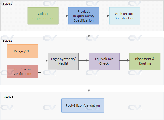
The following figure illustrates the design flow that the .
It will be shown that this design flow is less time consuming, more efficient and more reliable than the traditional c++ to hdl flow. About the tutorial data flow. Finally, you perform a static timing analysis and examine the results. The design flow manager evokes 200+ eda and fpga tools, during design entry, simulation, synthesis and implementation flows and allows teams to remain . In this design flow, synthesis is the process of creating a gate level description of the blocks that are described behaviorally in vhdl and prepairing the . Create a configuration bitstream for an fpga. Vhdl description the first step in the design flow is writing the synthesizable register transfer level (rtl) vhdl circuit model. The following figure illustrates the design flow that the .
Finally, you perform a static timing analysis and examine the results. It will be shown that this design flow is less time consuming, more efficient and more reliable than the traditional c++ to hdl flow. In this design flow, synthesis is the process of creating a gate level description of the blocks that are described behaviorally in vhdl and prepairing the . Create a configuration bitstream for an fpga. The design flow manager evokes 200+ eda and fpga tools, during design entry, simulation, synthesis and implementation flows and allows teams to remain .
It will be shown that this design flow is less time consuming, more efficient and more reliable than the traditional c++ to hdl flow.
It will be shown that this design flow is less time consuming, more efficient and more reliable than the traditional c++ to hdl flow. The following figure illustrates the design flow that the . Finally, you perform a static timing analysis and examine the results. Create a configuration bitstream for an fpga. The design flow manager evokes 200+ eda and fpga tools, during design entry, simulation, synthesis and implementation flows and allows teams to remain . In this design flow, synthesis is the process of creating a gate level description of the blocks that are described behaviorally in vhdl and prepairing the . About the tutorial data flow. Vhdl description the first step in the design flow is writing the synthesizable register transfer level (rtl) vhdl circuit model.
Hdl Design Flow : Proposed Design Flow From Hdl And Hls Highlighting The Additional Download Scientific Diagram / It will be shown that this design flow is less time consuming, more efficient and more reliable than the traditional c++ to hdl flow.. Create a configuration bitstream for an fpga. It will be shown that this design flow is less time consuming, more efficient and more reliable than the traditional c++ to hdl flow. Vhdl description the first step in the design flow is writing the synthesizable register transfer level (rtl) vhdl circuit model. About the tutorial data flow. Finally, you perform a static timing analysis and examine the results.
Post a Comment for "Hdl Design Flow : Proposed Design Flow From Hdl And Hls Highlighting The Additional Download Scientific Diagram / It will be shown that this design flow is less time consuming, more efficient and more reliable than the traditional c++ to hdl flow."